
Instruire & Consultanta
 Courses
2. Schematic Design (OrCAD)
2.1  OrCAD Capture, basic level
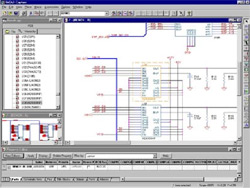
Course Contents
The course provides the participants with an overview of schematic design and presents, based on numerous case studies and examples, a practical approach on development of diagrams from electronic products. It presents fundamentals of schematic design and parts libraries creation. Some Flash movies, which are destined to a better understanding of schematic design flow, are also presented.
Course Duration
2 days - 1.5 days for the course and 0.5 day for performance evaluation, technical remarks and final discussions.
Course Outline
DAY 1
- Introduction in CAE-CAD-CAM. Basics of computer aided design in development of electronic products. Block diagram of a high performance CAE-CAD-CAM environment.
- The Capture work environment; project manager, schematic page editor, part editor, session log, toolbar & tool palette.
- Starting a project; creating and opening projects, designs, and libraries, working with files in a project, saving projects, designs, and libraries.
- Placing, editing, and connecting parts and symbols; placing and editing parts, searching for parts, working with power and ground symbols, placing and connecting wires.
- Adding and editing graphics and text.
- Libraries and parts; categories of libraries and parts. Creating and editing parts.
- Creating simple & complex designs; flat designs, hierarchical designs, concatenated (multi-page) designs.
DAY 2
- Preparing a SCM design for post-processing; annotating, visual checking, manual checking of a design.
- Basics of SCM post-processing.
- Interfacing Capture with Layout, SCM - PCB transfer, procedure and files.
- Optimizing the transfer based on ECO technique.
- Preparing the technical documentation of an electronic project.
- Course summary/review
- Multiple-choice test for the theory
- Practice exam
- Instructor/student conference with technical remarks and final discussions
Course Notes
A set of course notes and various printed technical documents will be provided to each participant.
Fee
500 EUR/company, unlimited number of participants
- For independent specialists the fee can be lower, based on negotiations.
Performance Evaluation
A final exam will be used at the end of the course to evaluate the performance. The exam is divided in two parts, one multiple-choice test for the theory and one practice exam focused on engineering aspects of the course.
Who should attend
The course is designed for electrical and electronics managers and leaders involved in supervising CAD schematic and PCB design, engineers, professors in the field of electronic packaging, and students who wish to get an overview of schematic design and to learn more about the design flow. The course is focused on various practical aspects and, due to a large number of examples which can be directly applied in practice, is addressed to people who want to learn quickly the basics of CAD schematic design.
2.2 OrCAD Capture, standard level
Course Contents
The course provides the participants with a systematic overview of schematic design and presents, based on numerous figures, case studies and examples, a practical approach on development of diagrams/schematics from electronic products. The chapters cover a large area of topics, from fundamentals of schematic design to complex hierarchical and multi-page projects. Some Flash movies, which are destined to a better understanding of schematic design flow, are also presented.
Course Duration
3 days - 2.5 days for the course and 0.5 day for performance evaluation, technical remarks and final discussions.
Course Outline
DAY 1
- Introduction in CAE-CAD-CAM. Basics of computer aided design in development of electronic products. Block diagram of high performance CAE-CAD-CAM environments.
- The Capture work environment; project manager, schematic page editor, part editor, session log, toolbar & tool palette.
- Starting a project; creating and opening projects, designs, and libraries, working with files in a project, saving projects, designs, and libraries.
- Setting up a project; defining preferences, setting up project template, defining title block information.
- Placing, editing, and connecting parts and symbols; placing and editing parts, searching for parts, working with power and ground symbols, placing and connecting wires and buses. Power & Ground (PWR & GND) of electronic circuits. Working with net alias and signals (underground/invisible connections).
- Adding and editing graphics and text; drawing lines, rectangles and squares, circles and ellipses, working with pictures, management of texts.
DAY 2
- Libraries and parts; categories of libraries and parts, part instances and occurrences, design cache. Creating and editing parts; parts and packages: homogeneous or heterogeneous, creating a new part, defining a part, power and ground terminals, invisible power pins, checking and saving a part, editing an existing part.
- Creating simple & complex designs; flat designs, hierarchical designs, concatenated (multi-page) designs, hierarchical blocks, ports, and pins, off-page connectors.
- Preparing a SCM design for post-processing; annotating, visual checking, manual checking of a design.
- SCM post-processing activities.
- Checking for design rules violations - DRC & ERC.
- Creating netlists for various purposes.
- Creating reports: bill of materials, cross reference, wirelist; printing a design.
DAY 3
- Interfacing Capture with Layout, SCM - PCB transfer; preparing a Capture design for use with Layout, creating a netlist for interfacing with Layout, general rules for a proper matching between SCM and PCB environments, working with PCB footprints for SCM parts, technological viewpoints.
- Using the Component Information System (CIS); basics of CIS, CIS work environment, using the CIS interface.
- Course summary/review
- Multiple-choice test for the theory
- Practice exam
- Instructor/student conference with technical remarks and final discussions
Course Notes
A set of course notes and various printed technical documents will be provided to each participant.
Fee
800 EUR/company, unlimited number of participants
- For independent specialists the fee can be lower, based on negotiations.
Performance Evaluation
A final exam will be used at the end of the course to evaluate the performance. The exam is divided in two parts, one multiple-choice test for the theory and one practice exam focused on engineering aspects of the course.
Who should attend
The course is designed for electrical and electronics engineers involved in schematic and PCB design, professors in the field of electronic packaging, technical managers, and students who wish to get a comprehensive overview of schematic design of electronic projects and to learn more about various applications. The course is focused on various practical aspects and, due to a large number of examples and case studies which can be directly applied in practice, is addressed also to R&D engineers and researchers from innovative companies involved in development of high performance electronic products.
2.3 OrCAD Capture, advanced level
Course Contents
The course provides the participants with a systematic overview of schematic design and presents, based on numerous figures, case studies and examples, a practical approach on development of diagrams from electronic products. The chapters cover a large area of topics, from fundamentals of schematic design to complex hierarchical and multi-page projects. Some Flash movies, which are destined to a better understanding of schematic design flow, are also presented. Additionally, high level topics, as aspects of technology, CIS, ECO, ITC, etc., are discussed.
Course Duration
4 days - 3 days for the course and 1 day for performance evaluation, technical remarks and final discussions.
Course Outline
DAY 1
- Introduction in CAE-CAD-CAM. Basics of computer aided design in development of electronic products. Block diagram of a high performance CAE-CAD-CAM environment. Integrated solutions for electronics industry.
- The Capture work environment; project manager, schematic page editor, part editor, session log, toolbar & tool palette.
- Starting a project; creating and opening projects, designs, and libraries, working with files in a project, saving projects, designs, and libraries, archiving a project.
- Setting up a project; defining preferences, setting up project template, defining title block information, creating a custom title block.
- Placing, editing, and connecting parts and symbols; placing and editing parts, searching for parts, working with power and ground symbols, placing and connecting wires and buses. Power & Ground (PWR & GND) of electronic circuits. Working with net alias and signals (underground/invisible connections). Using macros; Recording, playing, configuring a macro.
- Adding and editing graphics and text; drawing lines, rectangles and squares, circles and ellipses, working with pictures, management of texts.
DAY 2
- Libraries and parts; categories of libraries and parts, part instances and occurrences, design cache, primitive and non-primitive parts. Creating and editing parts; parts and packages: homogeneous or heterogeneous, creating a new part, defining a part, power and ground terminals, invisible power pins, checking and saving a part, editing an existing part, editing a part in a library, editing a part on a schematic page.
- Creating simple & complex designs; flat designs, hierarchical designs, concatenated (multi-page) designs, hierarchical blocks, ports, and pins, off-page connectors.
- Preparing a SCM design for post-processing; annotating, visual checking, manual checking of a design.
- SCM post-processing activities;
- Checking for design rules violations - DRC & ERC.
- Back annotating, re-annotating.
- Creating netlists for various purposes.
- Creating reports; bill of materials, cross reference, wirelist.
- Printing a design.
DAY 3
- Interfacing Capture with Layout, SCM - PCB transfer; preparing a Capture design for use with Layout, creating a netlist for interfacing with Layout, enabling inter-tool communication between Capture and Layout, general rules for a proper matching between SCM and PCB environments, working with PCB footprints for SCM parts, THD and SMD, technological viewpoints.
- Using the Component Information System (CIS); basics of CIS, CIS work environment, CIS explorer window, working with database parts, using the CIS interface, placing a database part on a schematic page, browsing part properties, linking a placed part to a database part.
DAY 4
- Course summary/review
- Multiple-choice test for the theory
- Practice exam
- Instructor/student conference with technical remarks and final discussions
Course Notes
A set of course notes and various printed technical documents will be provided to each participant.
Fee
1200 EUR/company, unlimited number of participants
- For independent specialists the fee can be lower, based on negotiations.
Performance Evaluation
A final exam will be used at the end of the course to evaluate the performance. The exam is divided in two parts, one multiple-choice test for the theory and one practice exam focused on engineering aspects of the course.
Who should attend
The course is designed for electrical and electronics engineers involved in schematic and PCB design, specialists, professors in the field of electronic packaging, technical managers, and students who wish to get a comprehensive overview of schematic design of electronic projects and to learn more about various applications. The course is focused on various practical aspects and, due to a large number of examples and case studies which can be directly applied in practice, is addressed also to R&D engineers and researchers from innovative companies involved in development of high performance electronic products.
| 1. Design and Complex Characterization of High Performance PCB Structures |
| 3. Circuit Simulation (PSpice) |